The demand by Cloud Data Centers for faster data delivery speeds at cost-effective prices is growing rapidly. Higher speeds are necessary for Cloud Data Centers to process the current explosion in traffic. Mobile and video use drove data center traffic to 4.7 zettabytes (ZB), or almost five trillion gigabytes (GB), in 2015, and Cloud traffic will hit 14.1ZB in 2020. Cisco predicts that in 2020, 92 percent of Data Center bandwidth will be used by cloud data workloads rather than traditional workloads. As expected, the requirements Cloud Data Centers have for resiliency and data redundancy when processing cloud data traffic necessitate high data transfer speeds.
The Need for Speed - but who is behind the wheel?
This need for speed is driven primarily by the large public cloud providers, such as Microsoft, Google, Facebook and Amazon. Analysts predict that the market for Data Center solutions will increase from an $18.6 billion market in 2015 to a $32.3 billion market in 2020. Solutions that also reduce operational cost through increased efficiency will be the most in demand.
Due to this enormous growth in traffic, Cloud Data Center operators are working to increase data delivery speeds from 100G to 400G as quickly as possible. But, there are considerations that must be made by these operators when evaluating solutions that can increase speed. These solutions will only work if they also reduce space requirements, power consumption and operational costs.
Solutions?
So, if space, power consumption and operational costs are a factor, the components (Lasers, Drivers, Amplifiers, PHYs etc.) going into these Cloud Data Centers must optimize these traits. One solution to the need for speed is the use of Etched Facet Technology (EFT) over traditional Cleaved Facet Technology (CFT). By utilizing EFT over CFT, manufacturers can offer smaller, more efficient and less expensive optical transceiver modules for optical interconnects used for high-speed data transfer at Cloud Data Centers.
EFT versus CFT
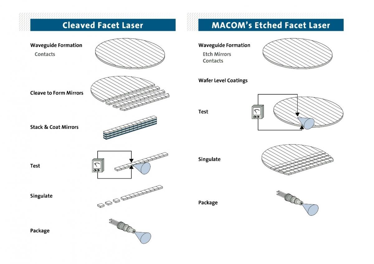
Figure 1. Source: Etched Facet Technology: Lighting the Path to 400G and Beyond in the Cloud Data Center
Let’s look at some of the reasons why EFT offers an effective solution to the need for speed. Lasers formed with the traditional CFT process are created from mechanically separated (or cleaved) wafers, and then stacked to create mirrors. EFT creates mirrors on the surface of the wafer using high-precision etching. Thus, there are many advantages to using EFT in manufacturing over CFT:
- EFT is a more precise process than CFT, therefore reducing the risk of defects due to cleaving.
- Testing when using CFT is expensive and can only be done at laser bar level. With EFT, testing can easily be done at a full wafer level, covering the whole range of temperatures.
- EFT provides an accurate location of the facet relative to alignment marks, whereas CFT cannot control the exact location of the facet. Using EFT, MACOM developed the proprietary self-alignment (SAEFT™) technology to attach lasers to silicon chips rather than using the slow active alignment process — thereby enabling more cost effectiveness at mass production levels.
- EFT allows high yield production of short cavity lasers, which is critical for high speed applications.
- EFT allows placing two lasers with a predetermined cavity length difference to increase the single mode yield.
- EFT can reduce laser beam divergence to increase fiber coupling efficiency.
- EFT can produce very low reflectivity facet by etching the facet at an angle, which is crucial for Semiconductor Optical Amplifier (SOA) applications.
- EFT can generate surface emission by etching the facet at an angle and custom angles, which is critical for Silicon Photonic (SiPh) chips with grating coupler.
- Non-hermetic passivation coating can be more effectively applied to EFT lasers on wafer scale, as compared to CFT lasers, which are coated on bar level.
Implementing the Advantages of Etched Facet Technology (EFT)
The advantages of EFT allow facets to be defined through high precision photolithography, rather than imprecise cleaving. This results in an unprecedented uniformity and yield, as well as the capability to build structures that are impossible to realize with conventional techniques. With no dependency on the crystallographic plane of the wafer, unique anti-reflection geometries can be used in place of expensive coatings.
Due to the EFT process, MACOM is able to more fully evaluate all of our lasers on the wafer in an automated, high-throughput test operation, in addition to dramatically reducing the cost of chip-handling. This process has enabled the integration of silicon PICs with lasers, creating the very first L-PIC™, or lasers integrated with a photonic integrated circuit. MACOM’s L-PIC enables a lower cost, efficient and high-yield data transfer solution, increasing the feasibility of adopting PICs as high density optical interconnect solutions for Cloud Data Centers.
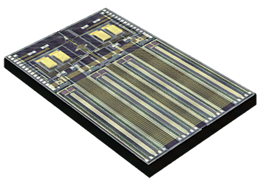
Figure 2: MACOM's L-PIC device combines four high-performance distributed feedback (DFB) laser diodes using MACOM's patented EFT, four 28G Mach-Zehnder optical modulators integrated with a coarse wavelength division multiplexer, monitor photodiodes and a high-performance output coupler for operation on one standard single mode fiber.
In cost-sensitive markets, solutions like MACOM’s EFT process enable high precision etching, minimize the risk of laser defects, reduce the overall cost of manufacturing lasers and offer a cost-effective and scalable solution, thereby delivering the products and solutions that will meet this upward need for speed.