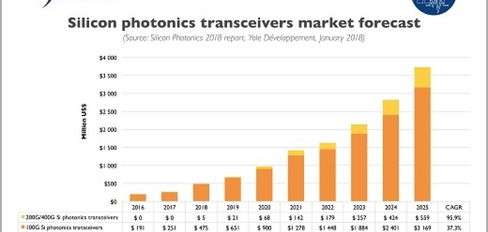
Silicon photonics is on the verge of experiencing dramatic uptake in optical transceivers, market research firm Yole Développement has reported, with the technology set to capture 35 per cent – almost $4 billion – of the optical transceiver market by 2025, up from just a few per cent in 2016.
The transceivers are expected to be used mostly for intra-data centre communication, according to Yole, with the strongest demand being for 400G (400 Gigabits per second), and 200G acting as an intermediate step between 100G and 400G.
Silicon photonics could capture almost $4 billion of the optical transceivers market by 2025. (Image: Yole Développement )
Silicon photonics is still a small market today, with sales at die level estimated to be $30 million in 2016, according to Yole. However, it has big promise, with a 2025 market value of $560 million at chip level and almost $4 billion at transceiver level.
‘The next evolution is to develop a 400G optical port over a single fibre across 500m at less than $1 per gigabit and with power <5mW/Gb,' commented Dr Eric Mounier, senior technology & market analyst at Yole.
One terabit per second rates should then follow, according to the market research firm.
Although the wafer area this accounts for will be a minute part of the worldwide SOI (silicon-on-insulator) market, it will represent significant value because of the SOI wafer high price.
In its new market report ‘Silicon Photonics’, Yole revealed the current status and future challenges for data centres, and explained why silicon photonics is the answer to future DC needs and other possible applications.
‘Silicon photonics technology has clearly reached its tipping point, with transceivers shipping in volume,’ the firm announced.
‘We believe we are only at the very beginning [of this increasing uptake] as there is massive ongoing development worldwide for further integration’, asserted Mounier. ‘The recent involvement of large integrated circuit foundries, such as TSMC’s relationship with Luxtera, and GlobalFoundries with Ayar Labs, are very encouraging signs showing the big promise for silicon photonics.
Further application
Telecom is also one possible application for silicon photonics, especially metropolitan networks from 80km to 1,500km in length, according to Yole. For example, Acacia Communications is developing coherent-based silicon photonics modules for telecom applications that reduce polarisation dispersion and losses while reducing channel passbands.
There is also interest for fibre-to-the-home (FTTH), where silicon photonics could be useful as FTTH moves from 10G to 25G, because more functionality will be needed such as wavelength tuning and switching.
Lastly, silicon photonics also has the potential to influence numerous other application areas, including biomedical sensing, lidar, and those in the aerospace/aeronautic industry.
‘Silicon photonics is at the maturity level of the electronics industry in the 1980s and there are still challenges to overcome,’ Yole concluded.
This story originally appeared on sister publication www.electrooptics.com
