Dutch start-up Effect Photonics says it is sampling its first products, a family of DWDM transceivers based on its low-cost optical ‘system-on-chip’ technology.
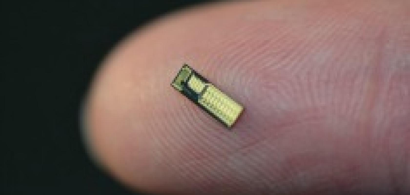
This technology integrates all the active and passive components of a DWDM transceiver within a single chip, without the traditional gold box packaging.
The announcement represents the culmination of more than five year’s work to commercialise technology originally developed at European universities (see Effect Photonics banks optical integration expertise).
“We’re excited to reach this milestone, which is to get the technology to market,” said James Regan, chief executive of Effect Photonics.
The company is targeting applications on the edge of the network where its technology is a good fit: namely, applications that require highly parallel but low-cost DWDM transceivers, such as 100G 80km transmission and optical access in residential and mobile networks.
One of the company’s first products will be a 100G 80km transceiver in an industry standard form factor. Today, this market can only be served by a coherent 100G product (for coherent, read expensive).
Andrew Schmitt, founder and analyst at Cignal Al, commented: “100Gb/s over 40km to 80km is a significant market opportunity that has no cost-effective solution today. This is the next battleground for 100G solutions.”
Effect Photonics claims that its fully integrated system-on-chip transceivers could be one third of the cost of products made using hybrid integration, which brings together different sub-components made from different materials, such laser arrays in one material, and a multiplexer in another.
Traditional multichannel optical transceivers are like Swiss watches, Regan says, where the individual sub-components have to be put together with very high precision and maintained in very high precision for the life of the device. This requires hermetically sealed, high-precision packaging – the gold box – in order to prevent failure at the many interfaces in the device.
In contrast Effect’s technology is based on a single chip so it’s very robust and stable, and doesn’t require hermetically sealed packages. “That’s only possible because there’s no free-space optics inside the module,” he added.
The starting point for a low-cost product is the concept of integration itself. “By combining functions you reduce the cost per function,” Regan explained. For example, Effect Photonics can put 10 lasers on a chip, either modulated directly or via Mach-Zehnder modulators, combined with an arrayed waveguide grating for multiplexing/demultiplexing and wavelength locking systems that give precise spectral control.
However, the key to being low cost is as much about the packaging as it is about the chip; a problem that’s vexed the optical components industry for years (see The problem with packaging). “We’ve designed the chip for the packaging and the packaging for the chip, to get advanced features at low cost,” Regan explained.
Eliminating the gold box, which is an expensive part in its own right, is a good first step. Further cost savings come from the fact that there’s very little labour content in the product; all the assembly processes are automated. “The packaging is very simple because all the real smarts are in the chip,” Regan explained.
He won’t reveal exactly how they’ve solved the packaging problem, except to say that “the technology we use is also used in a completely different industry to solve a completely different problem”.
The assembly and packaging will take place in Torbay, UK, a centre of excellence in optics, with its heritage from Nortel, Bookham, and Oclaro. The new approach to packaging means that skills are far more important to the company than plentiful low-cost labour. “This is all European built,” Regan added.
Effect Photonics will be showcasing its new product family at the forthcoming industry event OFC, booth no 2833, taking place in Anaheim, CA, on 20-24 March 2016.


