
Mathieu Bergont and Francois Couny look at the challenges that come with PIC testing and measurement
Photonic integrated circuits (PIC) are already deployed in commercial products and are steadily replacing traditional optical subassemblies, providing an improved level of miniaturisation while reducing electrical consumption. Data center interconnects (DCI) currently drive the demand for PIC, but 5G is also expected to benefit from PIC in the near future, indirectly affecting PIC testing and measurement requirements.
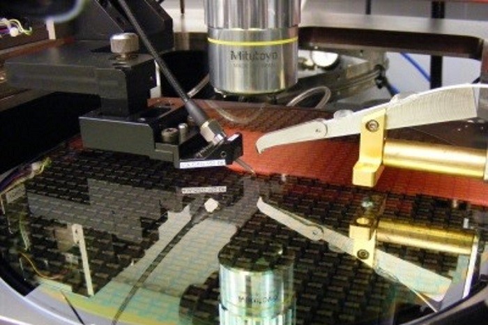
Optical PIC testing comes with several specific challenges, particularly at the early stage of manufacturing where the chips are individually tested on the wafer. At this stage, several sensitive components are characterised within each chip to determine if these critical components are within the specifications. This allows early detection of faulty components and prevents additional packaging-related costs. A non-exhaustive list of optical components found in PIC would include Mach-Zehnder modulators, AWGs and ring resonators.
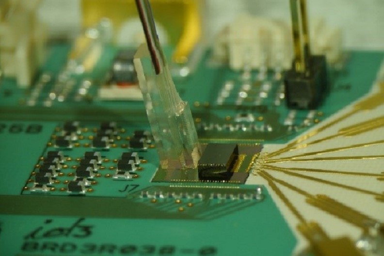
Testing at the wafer stage requires precise coupling of the light in and out of the chip to perform the required optical measurements; most frequently insertion loss. Fibre array including dozens of fibres are often used to couple the light in and out, reducing the number of alignments needed. Considering that each wafer consists of hundreds of chips, full characterisation of a wafer by qualified personnel may take up to a full day. Additionally, each chip may also require optical to electrical (O/E) measurements to characterize photodetectors, further complexifying the test procedure.
Additional testing is performed at a later stage in manufacturing when the chip is connected to its hybrid electronics. Functional measurements such as BER, eye diagram can be performed to validate the overall performances of the PIC subassembly.
Testing at the wafer stage is the most critical step and it is the bottleneck in manufacturing since hundreds of components must be quickly and reliably characterized. Reducing measurement time is key and this can be achieved by characterizing several channels simultaneously or by performing several measurements in parallel.
Many of the optical components within the PIC have sharp spectral features and high dynamic range which require the appropriate test equipment for accurate measurements. Among the different optical measurement techniques, tunable lasers offer both the highest resolution and dynamic range. Additionally, swept tunable lasers can achieve fast scanning speed without compromising the sampling resolution and dynamic range. A measurement time of a few seconds with a sampling resolution of 1pm and a 70-dB dynamic range is quite typical. High speed optical power meters are used after the device under test to measure the desired transfer function.
Our CTP10 component test platform is a multiport detection system that works in conjunction with the T100S-HP swept tunable laser to measure optical insertion loss and return loss. A modular platform like this can host up to 50 power meters, making it suitable for high port count devices such as AWGs and control several tunable lasers to perform measurements in parallel, increasing throughput and reducing test time.
Mathieu Bergont is product specialist and Francois Couny is product line manager at EXFO
